Treatment of transient problems in the power stage of integrated circuit
1.The product range of driving IC
IR company provides users with a variety of products from simple-phase to three-phase bridge driver IC. All types use high integrated electrical level conversion technology, simplifies the logic circuits controlling of the power MOS tube. The new product has been extended to have the ability to dirve 1200V power device.
As a cutting edge technology ,it can switch more current at a high speed. The adverse effects of stray parameters become more and more evident and attentive. The main purpose of this paper is to find their roots, quantitize the immunity ability of problems possiblly caused and finally obtain the greatest security zone.
2. Stray elements in bridge circuit
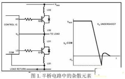
Figure 1 shows a typical IC driving bridge circuit composed of two MOSFET . In the power circuit, the device internal connections ,wireless inductance of uniform composition pins and the PCB line are represented by LS1.2 and LD1.2.
In addition, the stray parameter in the gate circuit should also be considered when wiring.Here we will mainly discuss the bridge circuit maximum current and the occurence of di/dt itself. In switching ,rapidly chaning current bridge circuit will provduce a voltage transients in the stray inductance. The transiention is coupled with other circuits,causing noise problem and increasing the switching loss, even in the worst condition damages IC.
3.The reason of undershoot
Becuase the problem is caused by the stray inductance, with the devices switching , as for driving IC ,the main problem is the VS may undershoot to rerence ground level. In contrast, forward undershoot generally does not cause problem. IR company has verified the IVIC technology has the advantage of high voltage resistance abillity.
The bridge circuits inductive load is perceptual,high end switches can cause the fact that sudden load current is converted to the low end freewheeling diode .Becuase the diodes opening is delayed , forward voltage drops and stray inductance LS1 and LD1 makes VS undershoot to the reference ground level.As shown in figure 1, during the dead time, if the load circuit can not be fully restored, when the low end devices is hard turned on, VS negative over shoot or oscillation occur.
4. VS undershoots effect on driving IC
IR driver IC gurantees that compared with COM, VS has at least 5V undershoot ability. If the negative overshoot is above that level, high output will be temporarily locked in its current state.
If VS is kept to an absolute maximum, IC will not be damaged. When the undershoot exceeds 5V, the high end output will not respond to the input control signal. The model shold be paid attention to . But in most applications, they can be ignored ,because with the switching events, high end usually do not require the quick changing state.
5. How to avoid locking
Appendix 1 shows the driver ICs typical internal parasitic diode structure. For any CMOS device, the diodes forward conduction or the reverse breakdown will cause the controllable thyristor tube to lock. The lockings ultimate consequences can be predicated . There may be temporarily the wrong job to complete destruction device.
Driver IC may be indirectly damaged by initial over stress reaction .For example, think that lock will make two outputs high and the bridge arm straight,which results in the damage of the device and then the IC.This failure mode may be the main reason of the damage of the driving IC and power device.


